Analog IC Note - Discharge Path
################ Statement ##############
## The series of Analog IC Note are ##
## the reviews of textbook or papers. ##
#######################################
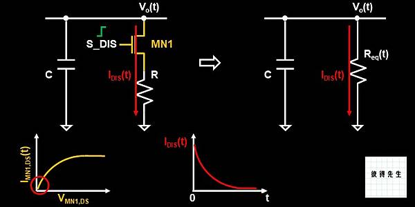
Sometime, we use a simple circuit composed of NMOS switch and POLY resistor for discharging a capacitor. Of course, NMOS switch acts as a control for activating the discharge function. POLY resistor gives the current-limiting function which prevents the too large rush current to the GND.

So, here are some points we should take care when designing this kind of thing.
1.Check the Max. rush current (IDIS) on spec and get the Vo(0).
Base on Ohm’s law, we get the Req(0) we need.
Req(0)=RMN1,ds(on)(0)+R. We can simulate RMN1,ds(on)(0) under VMN1,gs=(full swing) and VMN1,ds=Vo(0).
2.Remember to well design the width of NMOS and POLY resistor by the Max. rush current concern. You can find current density data in the material that the foundry offers.
3.Remind that there is a trade-off between suppression of rush current and the length discharge time.
4.Essentially, this circuit structure is a RC discharge circuit. The RC constant will determine the length of the discharge time.
5.The RMN1,ds(on) is meaningful only when t=0, because RMN1,ds(on)(t) varies during the discharging procedure.
I'm Peter, an analog IC R&D in Taiwan.
Nice to meet u.
-------------------------------------------------------------------
REF:
1. Sedra Smith,"Microelectronic Circuits",Edition 6
2. Charles K. Alexander and Matthew N.O. Sadiku, “Fundamentals of Electric Circuits”, Seventh Edition, McGraw Hill, 2021.


 留言列表
留言列表

